Home · Book Reports · 2018 · Fundamentals of Digital and Computer Design With VHDL

- Author :: Richard and Michael Sandige
- Publication Year :: 2011
- Read Date :: 2018-01-14
- Source :: (2011) Fundamentals_of_Digital_and_Computer_Design_with_VHDL.pdf
designates my notes. / designates important.
Thoughts
While reading this I watched, and worked, the first 90 or so lectures from the LBE Books VHDL youtube series.
This book contains a lot of pictures, truth tables, and waveforms. It is very easy to understand and I would recommend it highly for a first book. It is explicit, detailed, and includes lots of problems per chapter. Again, a great beginner book. I breezed through it in about a week.
The first part includes the foundational digital design topics you would expect: combinational logic, Karnaugh maps, flip flops, simple state machines/counters, and PALs, GALs, and C/PLDs. It spends some time on the design process and various hardware implementations.
The second part moves into computer design and is a change of pace from what I was looking for, but it is interesting none-the-less. The focus is on implementing simple computers in VHDL, not so much VHDL itself. This section builds slowly on the topics from the first section. Added to these foundational concepts are instruction sets, assembly language, program counters, and single I/O ports.
It starts off with the Harvard/RISC and Princeton/CISC machines and their simple block schematics. Next it introduces the basic computer explored in this section, Very Basic Computer 1 (VBC1), the assembly instruction for the VBC1, modules for input, output, registers, control logic, and the datapath. These are then combine debouncing, ALUs, shifting, and bitwise operations.
The third part simply expands on the second with VBC1-E, an enhanced version of the same computer designed in part two. VBC1-E adds more instructions, hardware and software interrupts, loadable memory, multiple I/O ports, and data memory
Each chapter concludes with dozens of problems, but there are no solutions for you to check your work. There is an appendix with 25+ detailed labs.
Table of Contents
- 01: Boolean Algebra, Boolean Functions, VHDL, and Gates
- 02: Number Conversions, Codes, and Function Minimization
- 03: Introduction to Logic Circuit Analysis and Design
- 04: Combinational Logic Circuit Design with VHDL
- 05: Bistable Memory Device Design with VHDL
- 06: Simple Finite State Machine Design with VHDL
- 07: Computer Circuits
- 08: Circuit Implementation Techniques
- 09: Complex Finite State Machine Design with VHDL
- 10: Basic Computer Architectures
- 11: Assembly Language Programming for VBC1
- 12: Designing Input/Output Circuits
- 13: Designing Instruction Memory, Loading Program Counter, and Debounced Circuit
- 14: Designing Multiplexed Display Systems
- 15: Designing Instruction Decoders
- 16: Designing Arithmetic Logic Units
- 17: Completing the Design for VBC1
- 18: Assembly Language Programming for VBC1-E
- 19: Designing Input/Output Circuits for VBC1-E
- 20: Designing the Data Memory Circuit for VBC1-E
- 21: Designing the Arithmetic, Logic, Shift, Rotate, and Unconditional Jump Circuits for VBC1-E
- 22: Designing a Circuit to Prevent Program Execution During Manual Loading for VBC1-E
- 23: Designing Extended Instruction Memory for VBC1-E
- 24: Designing the Software Interrupt Circuits for VBC1-E
- 25: Completing the Design for VBC1-E
· Chapter 01: Boolean Algebra, Boolean Functions, VHDL, and Gates
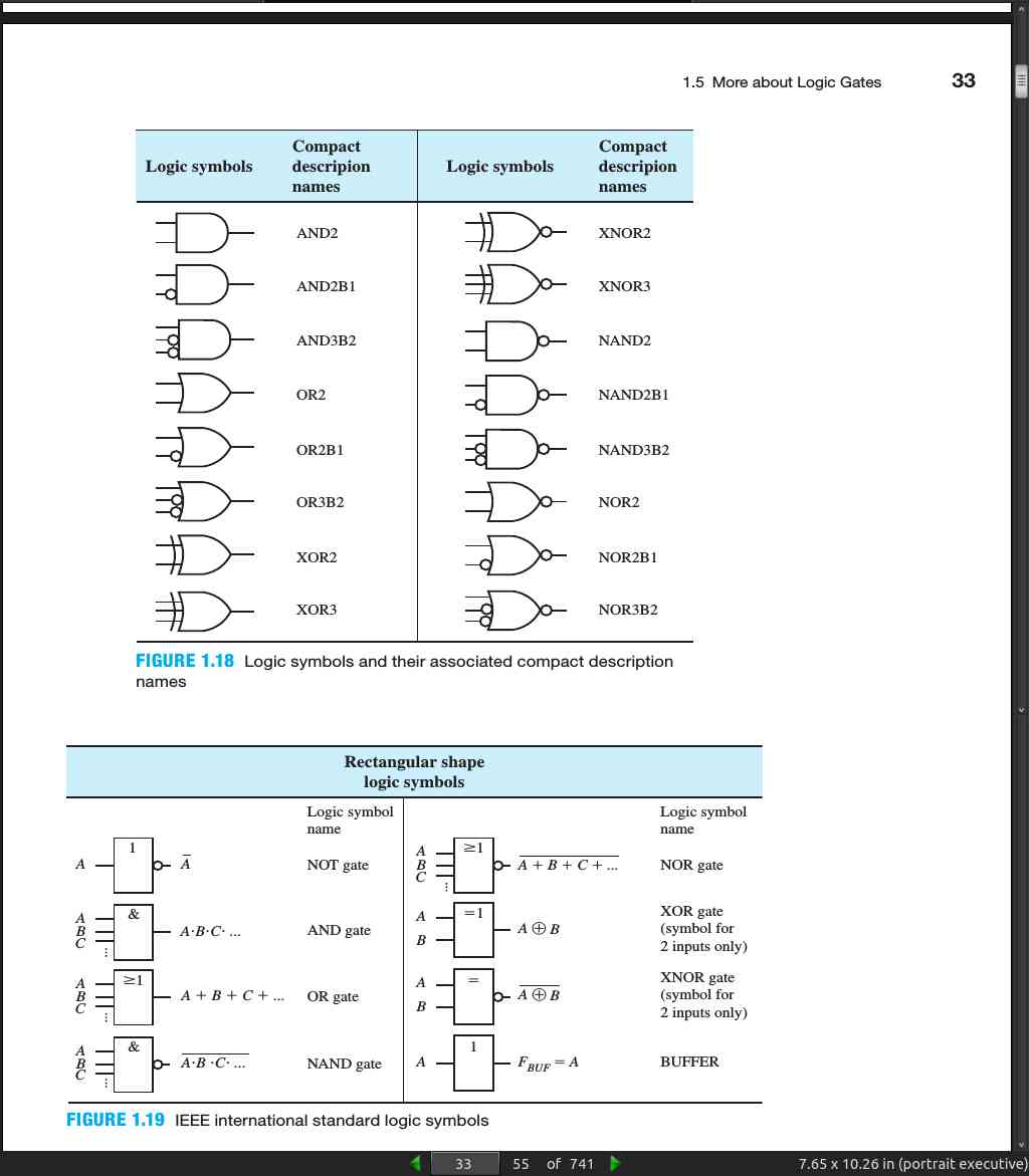
page 33:
· Chapter 02: Number Conversions, Codes, and Function Minimization
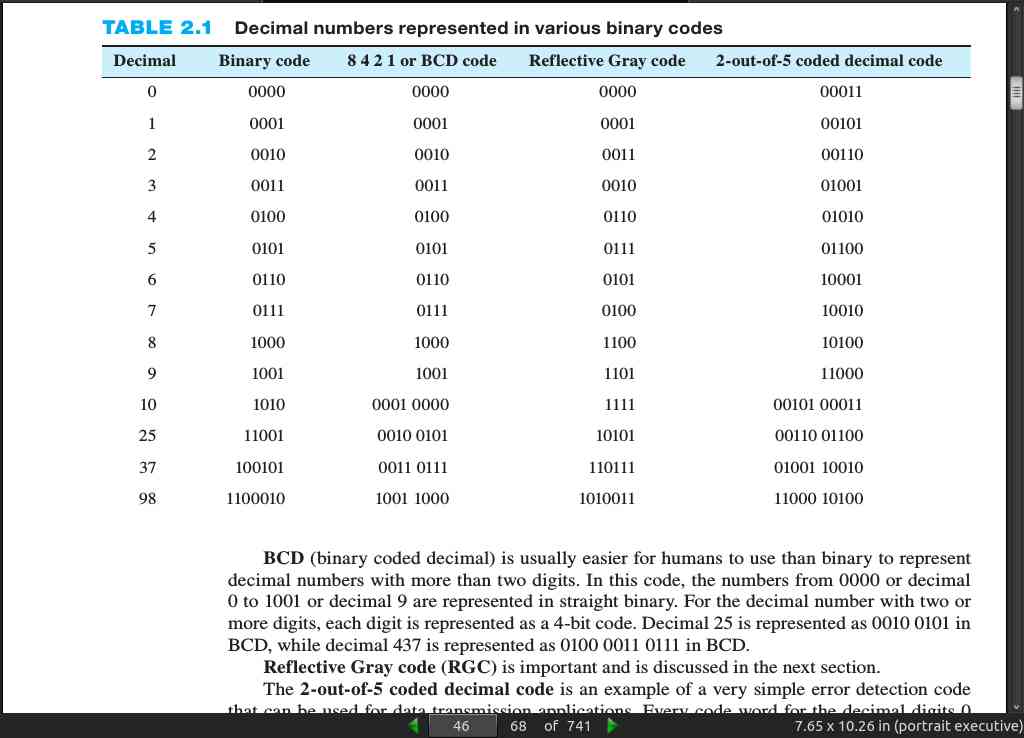
page 46:
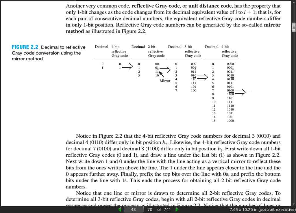
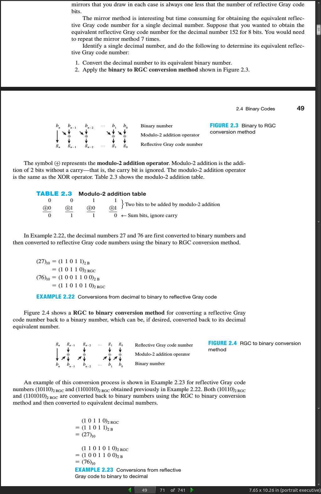
page 48:
- Notice in Figure 2.2 that the 4-bit reflective Gray code numbers for decimal 3 (0010) and decimal 4 (0110) differ only in bit position b2. Likewise, the 4-bit reflective Gray code numbers for decimal 7 (0100) and decimal 8 (1100) differ only in bit position b3 . First write down all 1-bit reflective Gray codes (0 and 1), and draw a line under the last bit (1) as shown in Figure 2.2. Next write down 1 and 0 under the line with the line acting as a vertical mirror to reflect these bits from the ones written above the line. The 1 under the line appears closer to the line and the 0 appears further away. Finally, prefix the top bits over the line with 0s, and prefix the bottom bits under the line with 1s.
page 49:
page 58:
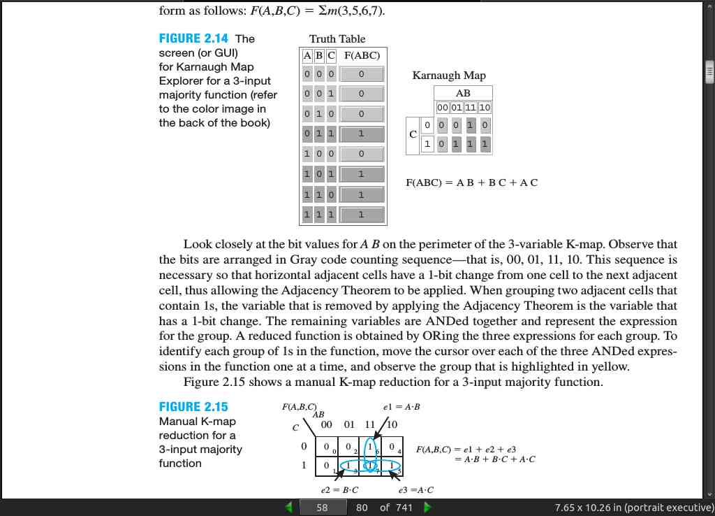
- Look closely at the bit values for A B on the perimeter of the 3-variable K-map. Observe that the bits are arranged in Gray code counting sequence—that is, 00, 01, 11, 10. This sequence is necessary so that horizontal adjacent cells have a 1-bit change from one cell to the next adjacent cell, thus allowing the Adjacency Theorem to be applied.
· Chapter 03: Introduction to Logic Circuit Analysis and Design
page 76:
- NAND and NOR gates are preferable to AND and OR gates. There are three reasons this is true: (1) NAND gates are generally faster than AND gates, and NOR gate are generally faster than OR gates in the same logic family; (2) NAND gates and NOR gates are available with a larger variety of fan-ins (gate inputs) to choose from than AND gates and OR gates; and (3) fewer IC packages are required to design circuits that use NAND gates and NOR gates because they are functionally complete gates
page 78:
- A nanosecond is one billionth of a second (or 10^-9 seconds) and is the time it takes for electricity to travel through a length of wire approximately 1 foot or about 1/3 meter.
page 85:
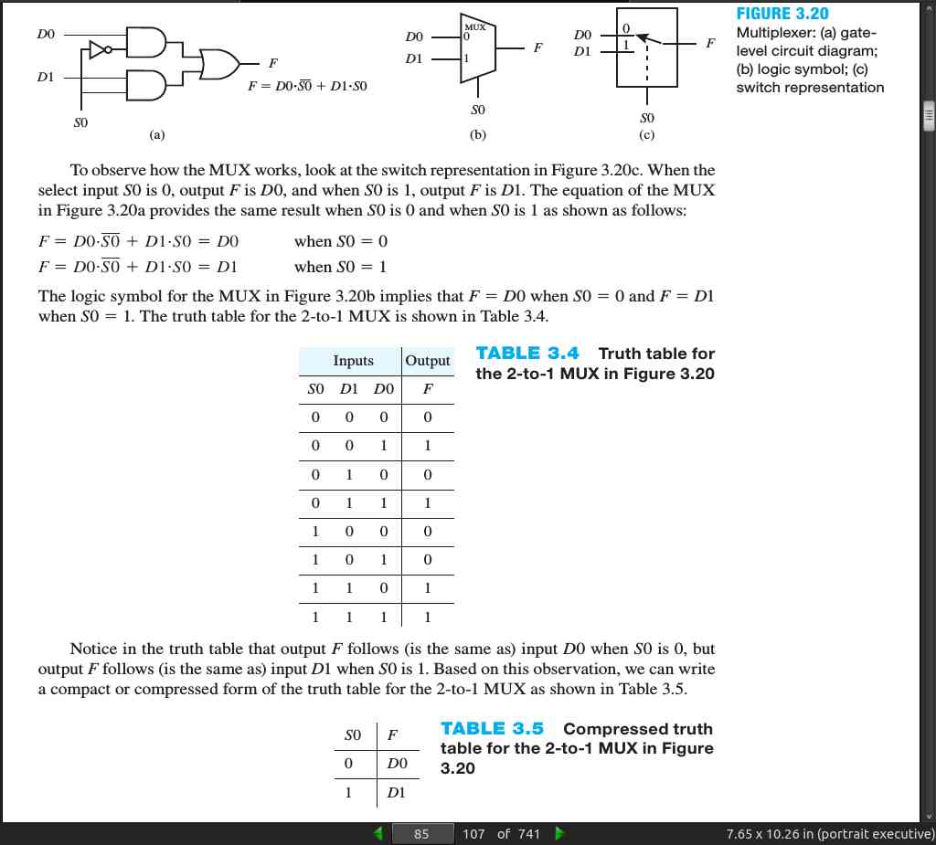
page 87:
- For a MUX design you need a 2^n-to-1 MUX for any n-variable function.
· Chapter 04: Combinational Logic Circuit Design with VHDL
page 118:
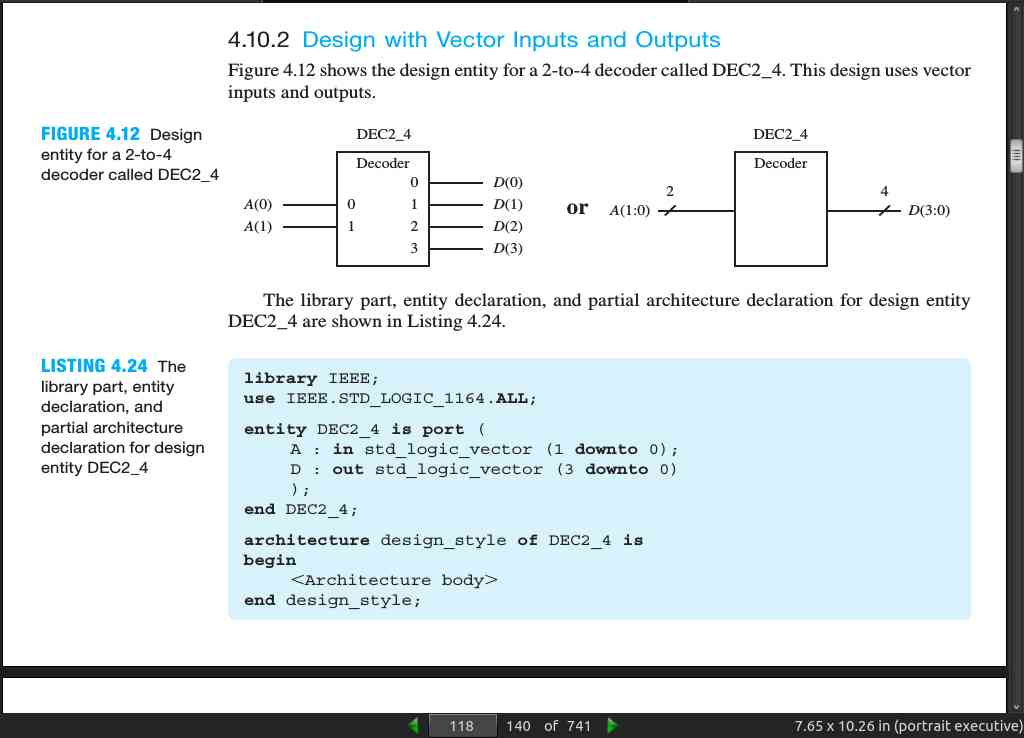
page 119:
library IEEE;
use IEEE.STD_LOGIC_1164.ALL;

entity DEC2_4 is port (
  A : in std_logic_vector (1 downto 0);
  D : out std_logic_vector (3 downto 0)
  );
end DEC2_4;

architecture design_style of DEC2_4 is
begin
  --<Architecture body>
end design_style;

--Boolean equations:
D(0) <= not A(1) and not A(0);
D(1) <= not A(1) and A(0);
D(2) <= A(1) and not A(0);
D(3) <= A(1) and A(0);

--Conditional signal assignment (CSA):
  D <= “0001” when A 5 “00” else
       “0010” when A 5 “01” else
       “0100” when A 5 “10” else
       “1000”;
  --Note: CSA is the concurrent equivalent of the if statement.

--Selected signal assignment (SSA):
with A select
  D <= “0001” when “00”,
    “0010” when “01”,
    “0100” when “10”,
    “1000” when “11”,
    “0001” when others;
  --Note: SSA is the concurrent equivalent of the case statement.

--If statement:
--place the if statement between begin and end process
  if    A = “00” then D <= “0001”;
  elsif A = “01” then D <= “0010”;
  elsif A = “10” then D <= “0100”;
  else D <= “1000”;
  end if;
  --Note: if statement is the sequential equivalent of the CSA.

--Case statement:
--place the case statement between begin and end process
case A is
  when “00” => D <= “0001”;
  when “01” => D <= “0010”;
  when “10” => D <= “0100”;
  when “11” => D <= “1000”;
  when others => null;
end case;
  --Note: case statement is the sequential equivalent of the SSA.
· Chapter 05: Bistable Memory Device Design with VHDL
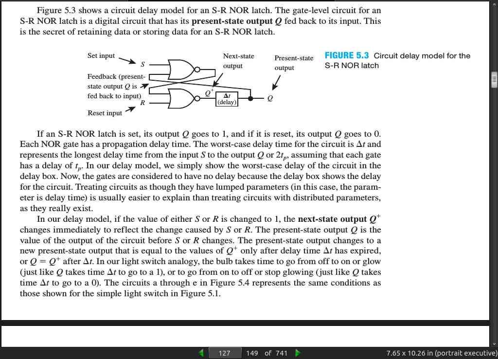
page 127:
page 128:
- Because the reset input overrides the set input, an S-R NOR latch circuit is referred to as reset dominant.
page 130:
- The rise time or fall time of a signal is usually defined as the time it takes the signal to change between the 10% and 90% values of the transition. The pulse width of a positive pulse is usually defined as the time it takes the signal to go from its 50% value on the rising edge of the pulse to its 50% value on the falling edge of the pulse.
page 131:
- The keyword
bufferis an alternate name that can be used for the keywordinoutfor signals that are not bidirectional.
page 131:
- To keep our VHDL code as simple as possible, we have elected to use mode
inoutthroughout the text to write our VHDL code for outputs that must also be feed back as inputs, because this results in fewer lines of code to type and also requires fewer variables
page 132:
- S-R NAND latch is set dominant rather than reset dominant like a basic S-R NOR latch.
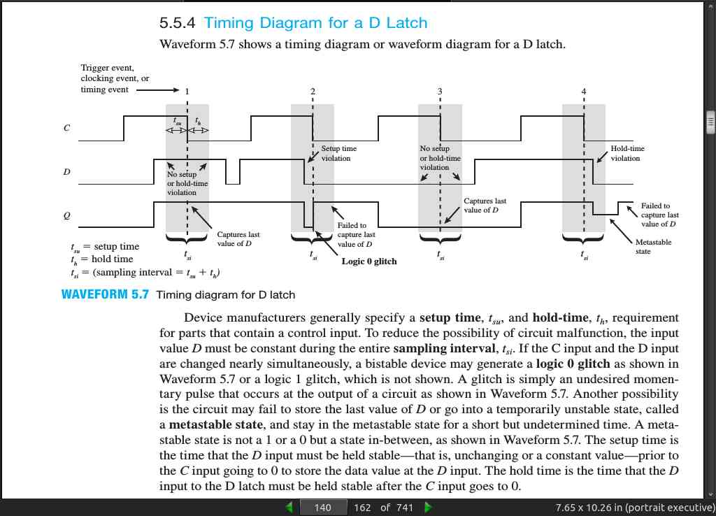
page 140:
page 142:
- never use external feedback around a D latch
· Chapter 06: Simple Finite State Machine Design with VHDL
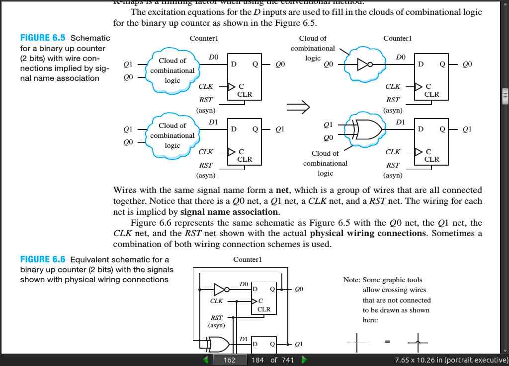
page 162:
page 173:
- Listing 6.7 shows the complete VHDL design for design entity ACCURATE_CLK_1HZ.
libraryIEEE;
use IEEE.STD_LOGIC_1164.ALL;
use IEEE.STD_LOGIC_UNSIGNED.ALL;

entity ACCURATE_CLK_1HZ is port (
  clk : in std_logic; --50 MHz clock
  slow_clk : inout std_logic
  );
end ACCURATE_CLK_1HZ;

architecture behavioral of ACCURATE_CLK_1HZ is
  signal count : integer;
  constant max_count: integer := 25000000;
  --25M clock cycles for half the period (0.5 s)

begin
  process (clk)
  begin
    if rising_edge(clk) then
      count <= count + 1;
      if count = max_count then
        slow_clk <= not slow_clk;
        count <= 0;
      end if;
    end if;
  end process;
end behavioral;
· Chapter 07: Computer Circuits
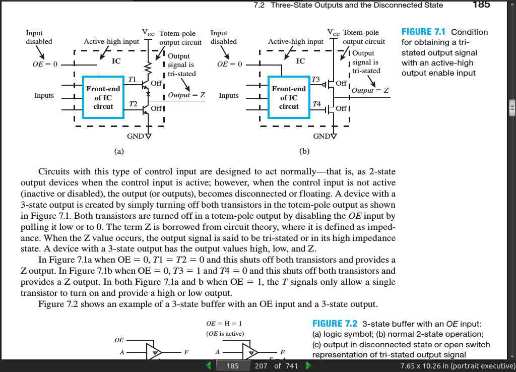
page 185:
- A device with a 3-state output is created by simply turning off both transistors in the totem-pole output as shown in Figure 7.1.
page 190:
- We obtain equivalent XOR gate symbols using an even number of bubbles. This may be remembered as the XOR even number of bubbles rule, even though XOR has an odd number of letters.
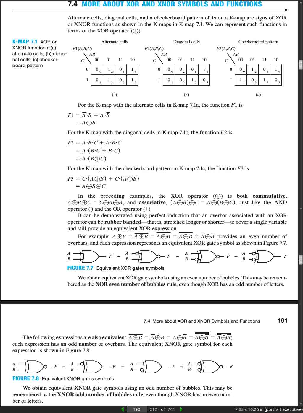
page 191:
-
We obtain equivalent XNOR gate symbols using an odd number of bubbles. This may be remembered as the XNOR odd number of bubbles rule, even though XNOR has an even number of letters.
-
An odd function has a value of 1 when the input string has an odd number of 1s (1,3,5, . . .), else it has a value of 0.
-
An even function has a value of 1 when the input string has an even number of 1s (0,2,4, . . .), else it has a value of 0.
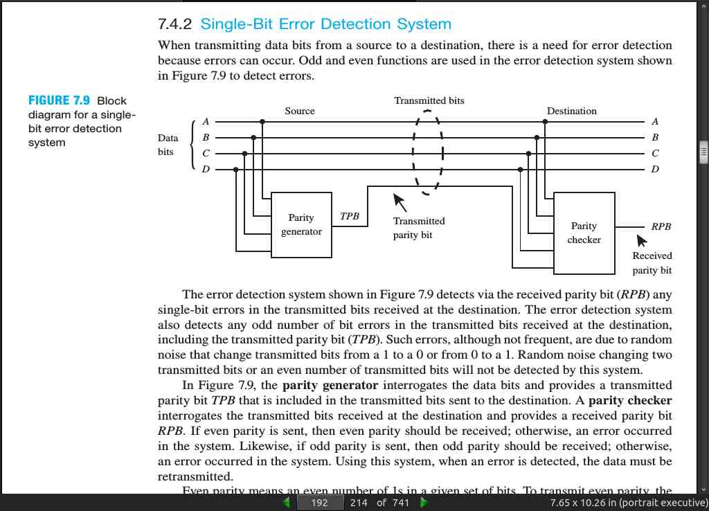
page 192:
page 194:
- Hamming codes can detect and correct single-bit errors. They can also detect but not correct double-bit errors.
page 201:
- -B = (2’s complement of B) = (1’s complement of B) + 1 = !B + 1, so A - B = A
- (-B) = A + (!B + 1) = A + !B + 1
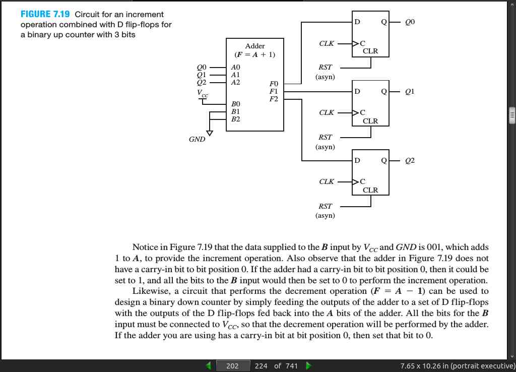
####### page 202:
· Chapter 08: Circuit Implementation Techniques
· Chapter 09: Complex Finite State Machine Design with VHDL
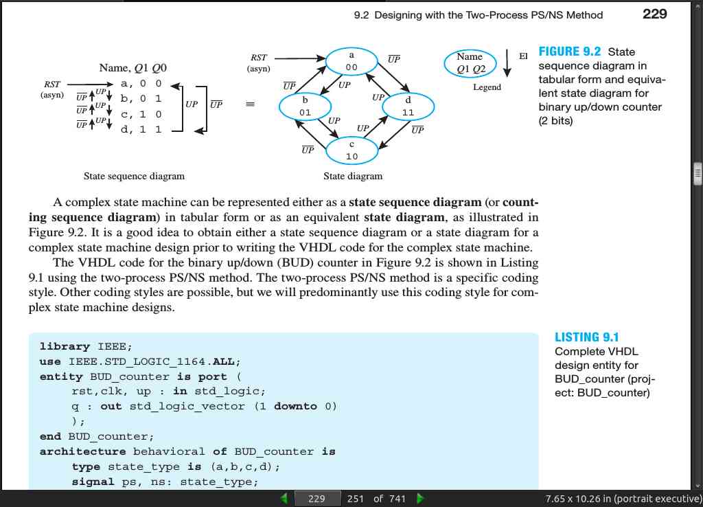
page 229:
library IEEE;
use IEEE.STD_LOGIC_1164.ALL;
entity BUD_counter is port (
  rst,clk, up : in std_logic;
  q : out std_logic_vector (1 downto 0)
  );
end BUD_counter;

architecture behavioral of BUD_counter is
  type state_type is (a,b,c,d);
  signal ps, ns: state_type; --present/next state

begin
--sync_proc:
process (rst,clk)
begin
  if rst = ‘1’ then ps <= a;
  elsif rising_edge (clk) then ps <= ns;
  end if;
end process;

--comb_proc:
process (ps,up)
begin
  case ps is
    when a => q <= “00”;
      if up = ‘1’ then ns <= b;
      else ns <= d;
      end if;
    when b => q <= “01”;
      if up = ‘1’ then ns <= c;
      else ns <= a;
      end if;
    when c => q <= “10”;
      if up = ‘1’ then ns <= d;
      else ns <= b;
      end if;
    when d => q <= “11”;
      if up = ‘1’ then ns <= a;
      else ns <= c;
      end if;
  end case;
end process;
end behavioral;
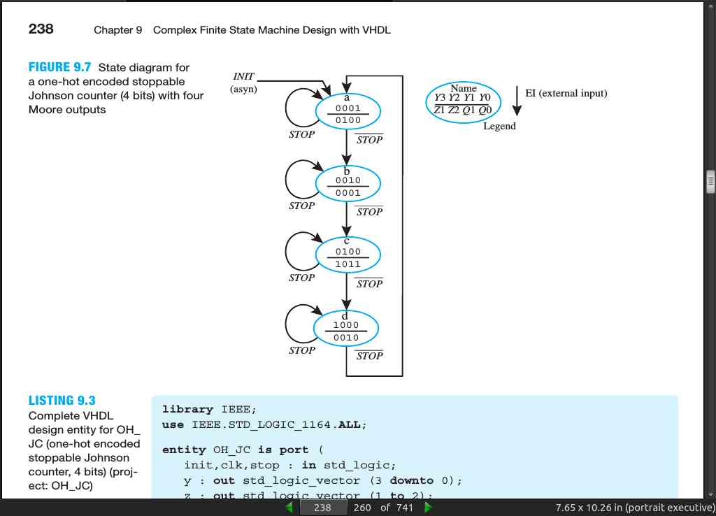
page 233:
-
This type of encoding style [one-hot encoding] is considered best for FPGAs that have an abundance of D flip-flops (or are register rich). With one dedicated flip-flop for each state, decoding logic is reduced for both the next-state functions and the output functions, and this encoding style can increase performance compared to using a compact or full encoding style for FPGAs.
-
Compact-encoded state machines generally require a minimum number of flip-flops and can require many gates. One-hot encoded state machines generally require a maximum number of flip-flops and just a few gates.
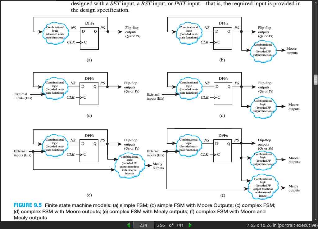
page 234:
page 238:
page 240:
library IEEE;
use IEEE.STD_LOGIC_1164.ALL;

entity OH_JC_MOD is port (
  init,clk,stop : in std_logic;
  y : out std_logic_vector (3 downto 0);
  z : out std_logic_vector (1 to 2);
  q : out std_logic_vector (1 downto 0)
  );
end OH_JC_MOD;

architecture mixed of OH_JC_MOD is
  type state_type is (a,b,c,d);
  signal ps, ns : state_type;

begin
--sync_proc:
process (init,clk)
begin
  if init 5 ‘1’ then ps <= a;
  elsif rising_edge (clk) then ps <= ns;
  end if;
end process;

--comb_proc:
process (ps,stop)
begin
  z <= “00”; q <= “00”; --default values for Moore outputs for case statement
  case ps is
    when a 5. z <= “01”; if stop 5 ‘1’ then ns <= a;
                         else ns <= b;
                         end if;
    when b 5. q <= “01”; if stop 5 ‘1’ then ns <= b;
                         else ns <= c;
                         end if;
    when c 5. q <= “11”; z <= “10”; if stop 5 ‘1’ then ns <= c;
                         else ns <= d;
                         end if;
    when d 5. q <= “10”; if stop 5 ‘1’ then ns <= d;
                         else ns <= a;
                         end if;
  end case;
end process;

with ps select
  y <= “0001” when a,
       “0010” when b,
       “0100” when c,
       “1000” when d;
end mixed;
-
The state variable Y or flip-flop outputs are provided in the selected signal assignment (SSA) after the combinational process. This tends to make the flip-flop output values easier to write because they are kept together in one selected signal assignment statement.
-
Observe that this design is a mixed architecture description because it contains both a behavioral design style and a dataflow design style in the same architecture description.
-
This is an alternate way of providing the state variable (or flip-flop) output values. If we decide later that we do not want to provide the state variable output values, we can simply comment out the selected signal assignment (SSA) without altering the combinational process (comb_proc).
· Chapter 10: Basic Computer Architectures
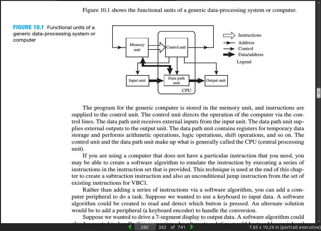
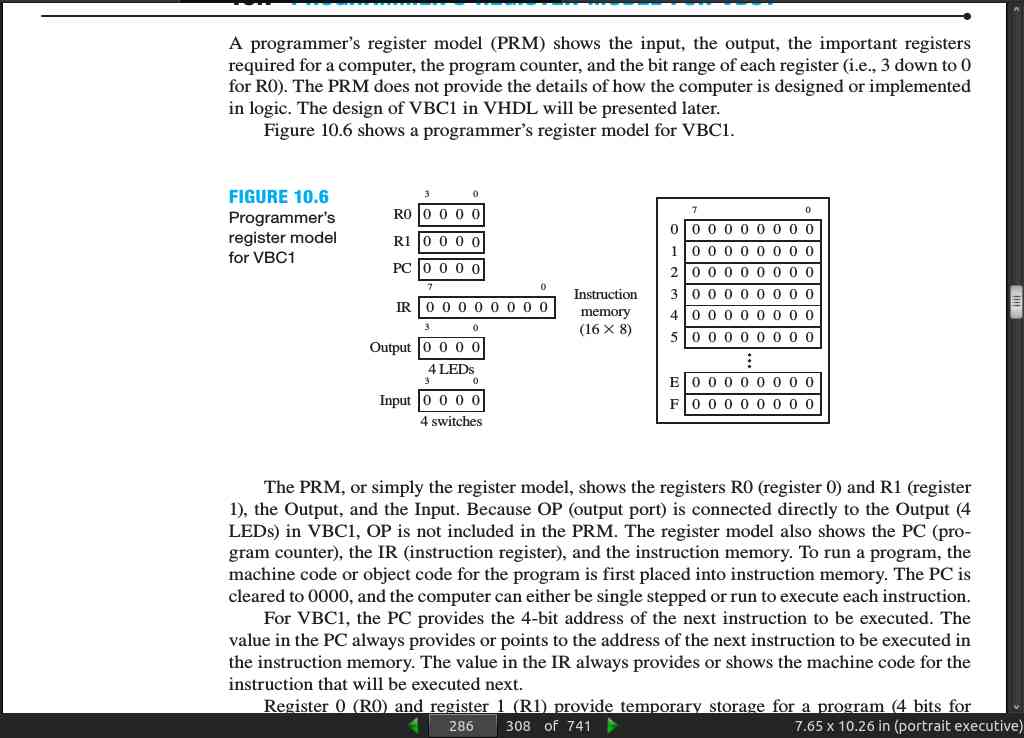
page 280:
page 283:
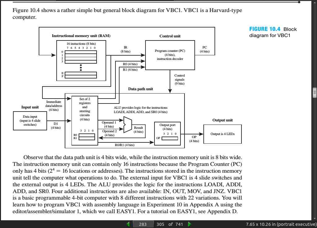
page 284:
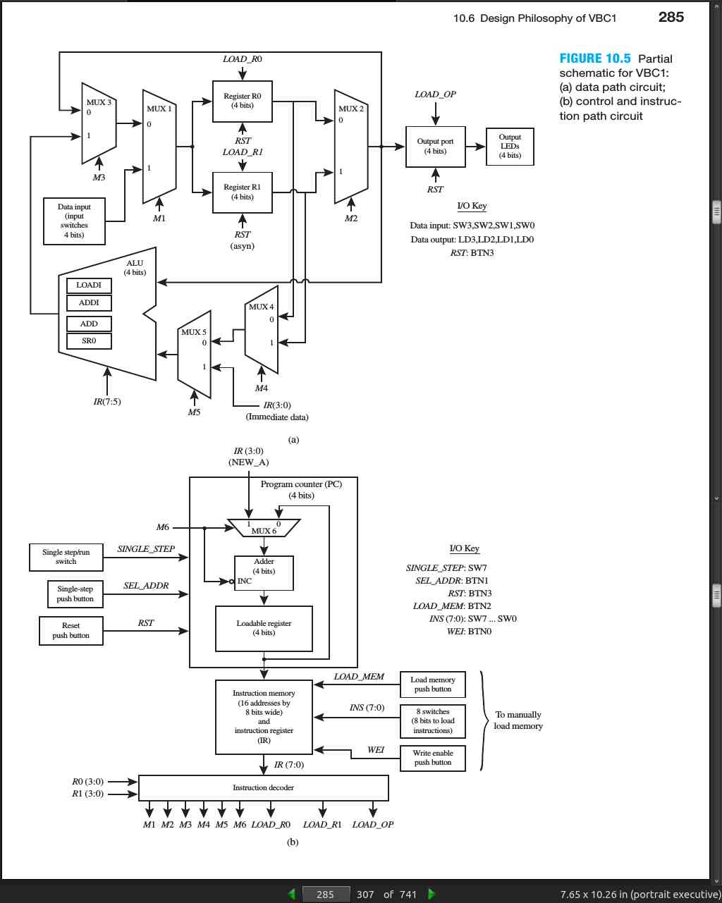
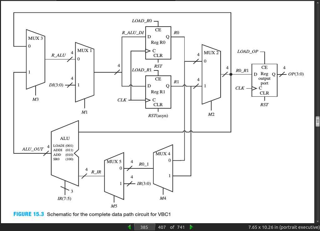
- Figure 10.5a can be described as follows:
MUXs (multiplexers) act as steering circuits.

Register R0 and register R1 are data registers with 4 bits.

MUXs 1, 2, and 3 provide the data path for the data registers labeled register
R0 and register R1.

The ALU is where the instructions LOADI, ADDI, ADD, and SR0 are implemented.

MUXs 2, 4, and 5 provide the data path for the two 4-bit operands supplied to
the ALU.

The block labeled Input switches 4 bits provides the data input.

The block labeled Output port drives the 4 LED outputs.
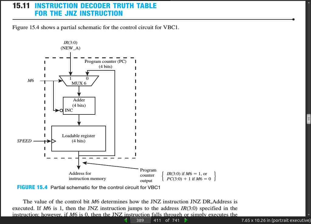
- The circuit in Figure 10.5b can be described as follows:
MUX 6 is enabled to allow the JNZ instruction to pass a new address to the
Adder in the program counter (PC).

If MUX6 is disabled, then the current value of the PC is incremented to point
to the next instruction.

The PC generates the address for the instruction memory, which is where the
instructions are placed.

The instruction memory provides the instructions for VBC1 via the instruction
register (IR). For this design, the instruction register is simply the current
contents of the instruction memory.

- The instruction decoder decodes the IR to provide the control for driving the
MUXs (1 through 6) and the data registers R0, R1, and the output port.

- The instructions IN, OUT, MOV, and JNZ are implemented by the way the circuit
is formed—that is, the architecture—controlled by the instruction decoder.
page 285:
page 286:
page 287:
page 288:
· Chapter 11: Assembly Language Programming for VBC1
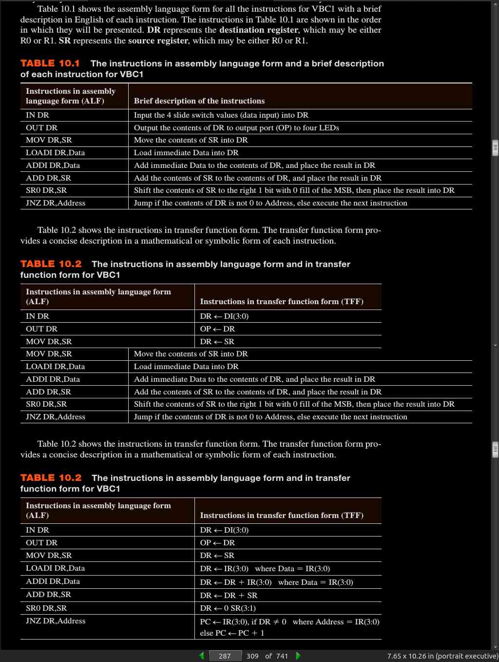
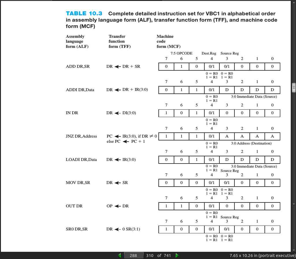
-
Overview of the VBC1 instruction set. IN, OUT, MOV, LOADI, ADDI, ADD, SR0, JNZ.
-
Samples of each instruction and a few “larger” example programs.
· Chapter 12: Designing Input/Output Circuits
page 316:
- A MUX (multiplexer) is a steering circuit. Another name for a MUX is a data selector because it selects or steers which input signal gets to the output of the MUX.
page 329:
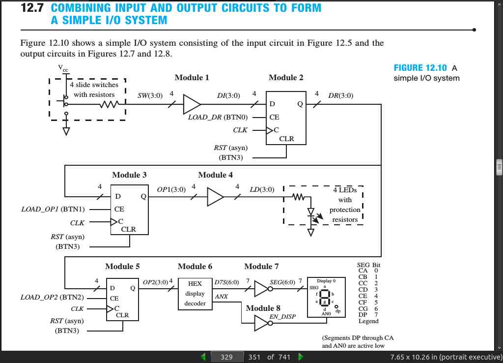
page 331:
- This documentation style, labeling modules and then stating which signals are between which modules makes it easier to read.
library IEEE;
use IEEE.STD_LOGIC_1164.ALL;

entity Simple_IO_System is port (
  sw : in std_logic_vector (3 downto 0);
  load_dr, clk, rst, load_op1, load_op2 : in std_logic;
  ld : out std_logic_vector (3 downto 0);
  seg : out std_logic_vector (6 downto 0);
  en_disp : out std_logic
  );
end Simple_IO_System;

architecture dataflow of Simple_IO_System is
--Modules 1 and 2 internal signal, di
  signal di: std_logic_vector (3 downto 0);
--Modules 2 and 3, Modules 2 and 5 internal signal, dr
  signal dr: std_logic_vector (3 downto 0);
--Modules 3 and 4 internal signal, op1
  signal op1: std_logic_vector (3 downto 0);
--Modules 5 and 6 internal signal, op2
  signal op2: std_logic_vector (3 downto 0);
--Modules 6 and 7 internal signal, d7s
  signal d7s: std_logic_vector (6 downto 0);
--Modules 6 and 8 internal signal, anx
  signal anx: std_logic;
begin
--Module 1 code, buffer
  di <= sw;
--Module 2 code, loadable DFFs with a clear input
  dr <= “0000” when rst = ‘1’ else
            di when load_dr = ‘1’ and rising_edge (clk);
--Module 3 code, loadable DFFs with a clear input
  op1 <= “0000” when rst = ‘1’ else
             dr when load_op1 =’1’ and rising_edge (clk);
--Module 4 code, buffer
  ld <= op1;
--Module 5 code, loadable DFFs with a clear input
  op2 <= “0000” when rst = ‘1’ else
             dr when load_op2 = ‘1’ and rising_edge (clk);
--Module 6 code, HEX display decoder
  d7s <= “0111111” when op2 = “0000” else
         “0000110” when op2 = “0001” else
         “1011011” when op2 = “0010” else
         “1001111” when op2 = “0011” else
         “1100110” when op2 = “0100” else
         “1101101” when op2 = “0101” else
         “1111101” when op2 = “0110” else
         “0000111” when op2 = “0111” else
         “1111111” when op2 = “1000” else
         “1101111” when op2 = “1001” else
         “1110111” when op2 = “1010” else
         “1111100” when op2 = “1011” else
         “0111001” when op2 = “1100” else
         “1011110” when op2 = “1101” else
         “1111001” when op2 = “1110” else
         “1110001”;
  anx <= ‘1’;
--Module 7 code, NOT gates
  seg <= not d7s;
--Module 8 code, NOT gate
  en_disp <= not anx;
end dataflow;
page 332:
- Alternate design for module 2:
--Module 2 code, loadable DFFs with a clear input
process (rst, clk)
begin
  if rst = ‘1’ then dr <= “0000”;
  elsif rising_edge (clk) then
    if load_dr = ‘1’ then dr <= di;
    end if;
  end if;
end process;
- Alternate design for module 3:
--Module 3 code, loadable DFFs with a clear input
process (rst, clk)
begin
  if rst = ‘1’ then op1 <= “0000”;
  elsif rising_edge (clk) then
    case load_op1 is
      when ‘1’ => op1 <= dr;
      when ‘0’ => op1 <= op1;
      when others => null;
    end case;
  end if;
end process;
page 333:
- Alternate design for module 5:
--Module 5 code, loadable DFFs with a clear input
process (rst, clk)
begin
	case rst is
	  when ‘1’ => op2 <= “0000”;
	  when ‘0’ => if rising_edge(clk) then
	                case load_op2 is
	                  when ‘1’ => op2 <= dr;
	                  when ‘0’ => op2 <= op2;
	                  when others => null;
	                end case;
	              end if;
	  when others => null;
	end case;
end process;
· Chapter 13: Designing Instruction Memory, Loading Program Counter, and Debounced Circuit
page 335:
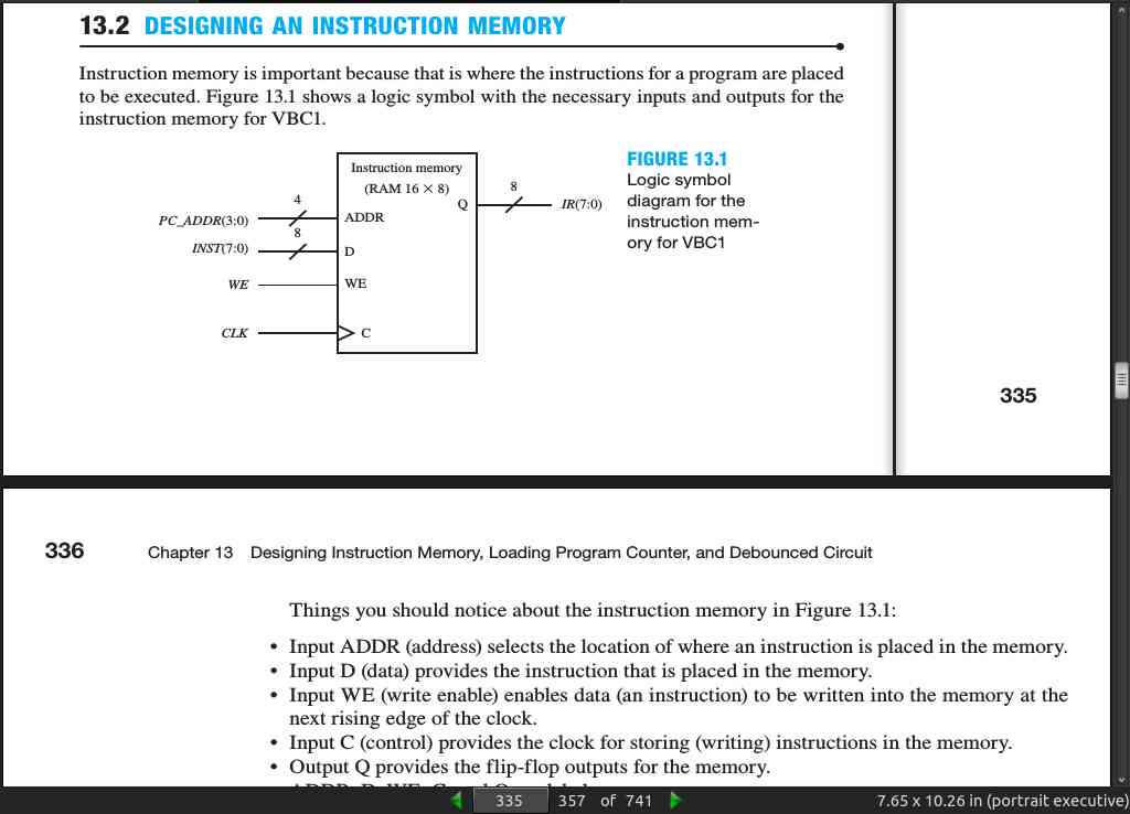
page 336:
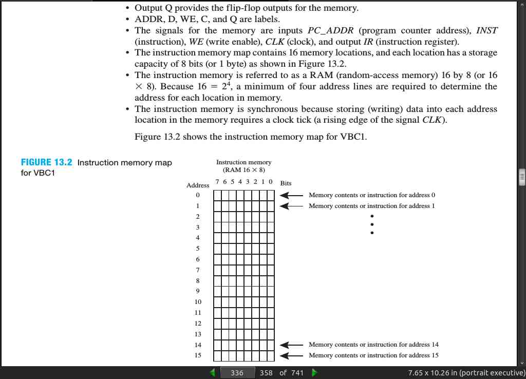
page 337:
library IEEE;
use IEEE.STD_LOGIC_1164.ALL;
use IEEE.STD_LOGIC_UNSIGNED.ALL;

entity instruction_memory is port (
  pc_addr : in std_logic_vector (3 downto 0);
  inst : in std_logic_vector (7 downto 0);
  we, clk : in std_logic;
  ir : out std_logic_vector (7 downto 0)
  );
end instruction_memory;

architecture Mixed of instruction_memory is
  type mem_type is array (0 to 15) of std_logic_vector (7 downto 0);
  signal mem : mem_type;

begin
process (clk)
begin
  if rising_edge (clk) then
    if we = ‘1’ then mem (conv_integer (pc_addr)) <= inst;
    end if;
  end if;
end process;

  ir <= mem (conv_integer (pc_addr));
end Mixed;
page 339:
- Alternate instruction memory module. ir <= mem is placed inside the process and mem is added to the sensitivity list.
library IEEE;
use IEEE.STD_LOGIC_1164.ALL;
use IEEE.STD_LOGIC_UNSIGNED.ALL;

entity instruction_memory_mod is port (
  pc_addr : in std_logic_vector (3 downto 0);
  inst : in std_logic_vector (7 downto 0);
  we, clk : in std_logic;
  ir : out std_logic_vector (7 downto 0)
  );
end instruction_memory_mod;

architecture Behavioral of instruction_memory_mod is
  type mem_type is array (0 to 15) of std_logic_vector (7 downto 0);
  signal mem : mem_type;

begin
process (clk, mem)
begin
  if rising_edge (clk) then
    if we = ‘1’ then mem (conv_integer (pc_addr)) <= inst;
    end if;
  end if;
  ir <= mem (conv_integer (pc_addr));
end process;
end Behavioral;
page 340:
- To load a program at startup into instruction memory: (must zero unused addresses)
type mem_type is array (0 to 15) of std_logic_vector (7 downto 0);
signal mem: mem_type := (
  --stoppable 4-bit binary-up counter program
    X”20”, X”c0”, X”b0”, X”f2”,X”61”, X”e1”, X”21”, X”e0”,
    X”00”, X”00”, X”00”, X”00”, X”00”, X”00”, X”00”, X”00”);
page 342:
- Easier way to read the loaded program:
type mem_type is array (0 to 15) of std_logic_vector (7 downto 0);
signal mem: mem_type :5 (
      -- ; robot eye program
      -- ; inline programming, i.e., no internal loops
      --
X"31",-- start: loadi r1,1
X"d0",-- out r1
X"32",-- loadi r1,2
X"d0",-- out r1
X"34",-- loadi r1,4
X"d0",-- out r1
X"38",-- loadi r1,8
X"d0",-- out r1
X"34",-- loadi r1,4
X"d0",-- out r1
X"32",-- loadi r1,2
X"d0",-- out r1
X"f0",-- jnz r1, start
      --
X"00",X"00",X"00");
page 346:
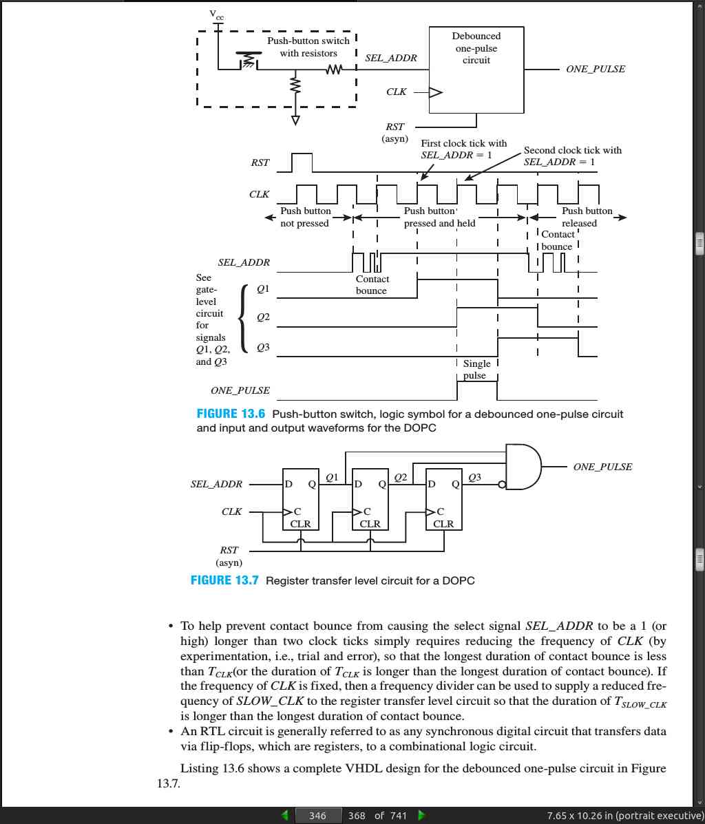
page 347:
- Simple debounce circuit (needs clk to be slow, about 10ms).
library IEEE;
use IEEE.STD_LOGIC_1164.ALL;

entity debounced_OPC is port (
  rst, clk, sel_addr : in std_logic;
  Q1, Q2, Q3 : inout std_logic;
  one_pulse : out std_logic
  );
end debounced_OPC;

architecture Mixed of debounced_OPC is
begin
  process (rst, clk)
  begin
    if rst = ‘1’ then
      Q1 <= ‘0’; Q2 <= ‘0’; Q3 <= ‘0’;
    elsif (clk’event and clk 5 ‘1’) then
      Q1 <= sel_addr;
      Q2 <= Q1; Q3 <= Q2;
    end if;
  end process;
    one_pulse <= Q1 and Q2 and not Q3;
end Mixed;
- The internal signals Q1, Q2, and Q3 are placed in the entity, so they can be displayed in the simulation.
page 354:
- Clock skew is the delay of the clock signal to a flip-flop from the clock source such that all flip-flops are not triggered at the same time, as they should be.
· Chapter 14: Designing Multiplexed Display Systems
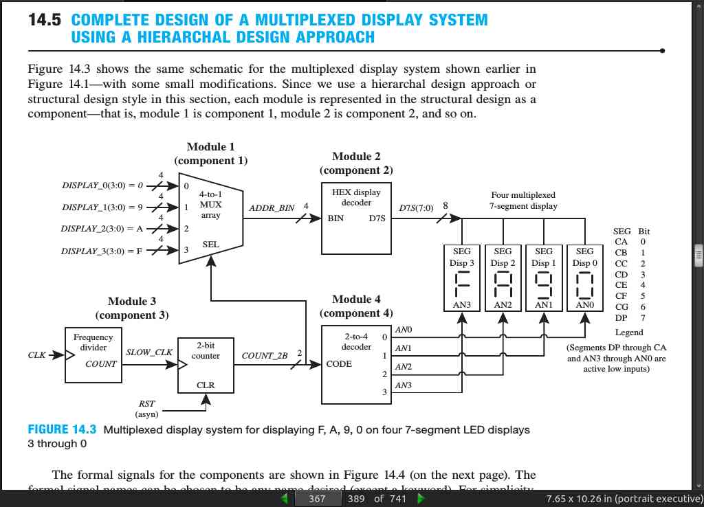
page 367:
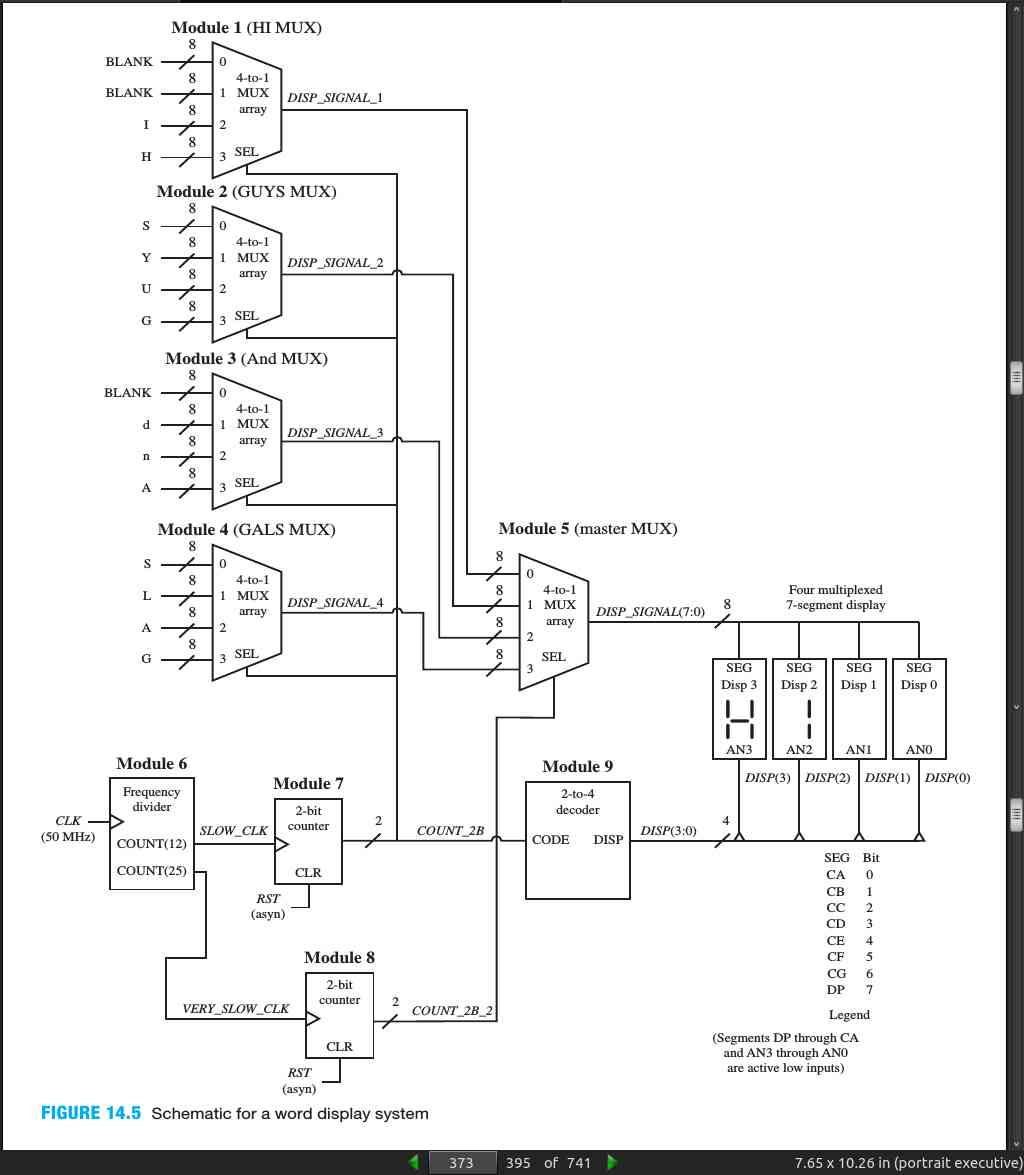
page 373:
· Chapter 15: Designing Instruction Decoders
page 382:
- To design an instruction decoder, we recommend using Procedure ID, which is listed as follows: (1) use a process with a case statement to select each instruction by its OPCODE, (2) specify the default instruction decoder output values before the case statement, and (3) use Boolean equations for the control bits within the case statement. (Note: Only the control bits that are different from the default instruction decoder output values need to be added to the case statement.)
page 383:
process (ir)
begin
  --default instruction decoder output values
  m1 <= ‘0’; m2 <= ‘0’; m3 <= ‘0’;
  load_r0 <= ‘0’; load_r1 <= ‘0’; load_op <= ‘0’;
  case ir (7 downto 5) is
    --for the IN instruction
    when “101” => m1 <= ‘1’;
                 load_r0 <= not ir(4);
                 load_r1 <= ir(4);
    when others =>. null;
  end case;
end process;
page 386:
page 389:
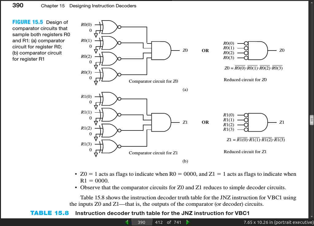
page 390:
page 391:
- JNZ:
process (ir, r0, r1)
begin
  --default instruction decoder output values
  m1 <= ‘0’; m2 <= ‘0’; m3 <= ‘0’; m4 <= ‘0’; m5 <= ‘0’;
  m6 <= ‘0’; load_r0 <= ‘0’; load_r1 <= ‘0’; load_op <= ‘0’;
  case ir (7 downto 5) is
    --for the JNZ instruction
    when “111” => m6 <= (not ir(4) and (r0(0) or r0(1) or
                         r0(2) or r0(3))) or (ir(4) and (r1(0)
                         or r1(1) or r1(2) or r1(3)));
    when others => null;
  end case;
end process;
page 392:
- Alternate JNZ:
process (ir, r0, r1)
begin
  --default instruction decoder output values
  m1 <= ‘0’; m2 <= ‘0’; m3 <= ‘0’; m4 <= ‘0’; m5 <= ‘0’; m6 <= ‘0’;
  load_r0 <= ‘0’; load_r1 <= ‘0’; load_op <= ‘0’;
  case ir (7 downto 5) is
	  --for the JNZ instruction
    when “111” =>
      if ir(4) = ‘0’ then
        if r0 /= “0000” then
          m6 <= ‘1’;   --jump
        else m6 <= ‘0’;--increment
        end if;
      elsif ir(4) = ‘1’ then
        if r1 /= “0000” then
          m6 <= ‘1’;    --jump
        else m6 <= ‘0’; --increment
        end if;
      end if;
    when others => null;
  end case;
end process;
page 393:
- a general format or template for the instruction decoder for VBC1.
process (ir, r0, r1)
begin
  --put default instruction decoder output values here, e.g., m1 <= ‘0’ m2 <=
  --‘0’, etc.
  case IR (7 downto 5) is--the OPCODE for each instruction is in bits (7:5) in the IR

    --the IN instruction has the OPCODE 101
    when “101” => --put output equations for the IN instruction here

    --the OUT instruction has the OPCODE 110
    when “110” => --put output equations for the OUT instruction here

    --the MOV instruction has the OPCODE 000
    when “000” => --put output equations for the MOV instruction here

    --the LOADI instruction has the OPCODE 001
    when “001” => --put output equations for the LOADI instruction here

    --the ADDI instruction has the OPCODE 011
    when “011” => --put output equations for the ADDI instruction here

    --the ADD instruction has the OPCODE 010
    when “010” => --put output equations for the ADD instruction here

    --the SR0 instruction has the OPCODE 100
    when “100” => --put output equations for the SR0 instruction here

    --the JNZ instruction has the OPCODE 111
    when “111” => --put output equations for the JNZ instruction here
    when others => null;
  end case;
end process;
· Chapter 16: Designing Arithmetic Logic Units
page 401:
- ADD instruction in ALU:
alu_process:
process (ir(7 downto 5), r0_r1, r_ir)
begin
  alu_out <= “0000”; --default value to prevent creating
                     --inferred latches
  case ir(7 downto 5) is
    when “010” => alu_out <= r0_r1 1 r_ir; --ADD
    when others => null;
  end case;
end process;
page 402:
- General ALU layout:
process (ir(7 downto 5), r0_r1, r_ir)
begin
  alu_out <= “0000”; --default value to prevent creating inferred latches
  case ir(7 downto 5) is --the OPCODE for each ALU instruction is in bits (7:5) in
                         --the IR

  --the LOADI instruction has the OPCODE 001
  when “001” => --enter the ALU output equation for the LOADI instruction here

  --the ADDI instruction has the OPCODE 011
  when “011” => --enter the ALU output equation for the ADDI instruction here

  --the ADD instruction has the OPCODE 010
  when “010” => --enter the ALU output equation for the ADD instruction here

  --the SR0 instruction has the OPCODE 100
  when “100” => --enter the ALU output equation for the SR0 instruction here
  when others => null;
  end case;
end process;
· Chapter 17: Completing the Design for VBC1
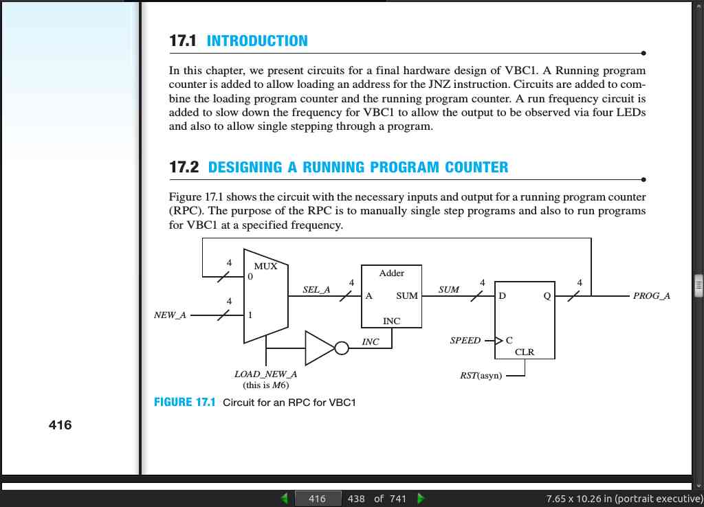
page 416:
· Chapter 18: Assembly Language Programming for VBC1-E
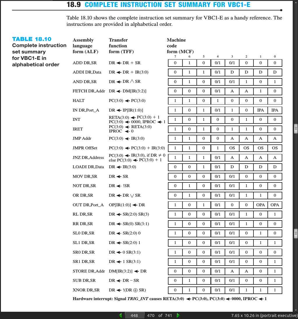
page 448:
· Chapter 19: Designing Input/Output Circuits for VBC1-E
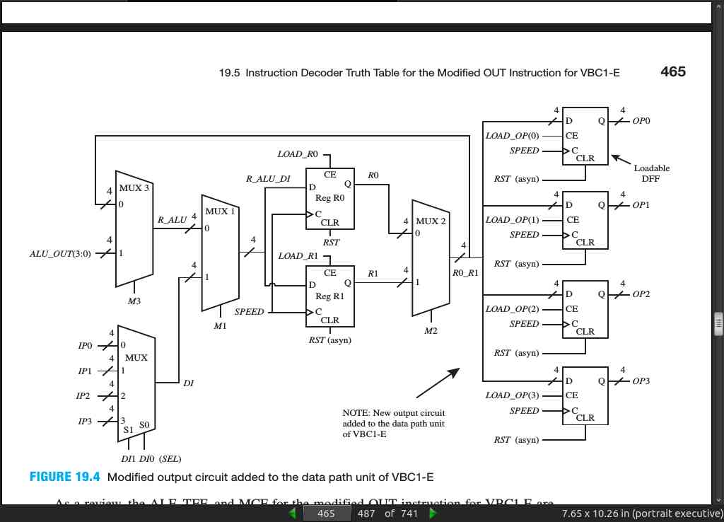
page 465:
· Chapter 20: Designing the Data Memory Circuit for VBC1-E
· Chapter 21: Designing the Arithmetic, Logic, Shift, Rotate, and Unconditional Jump Circuits for VBC1-E
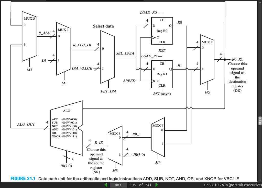
page 483:
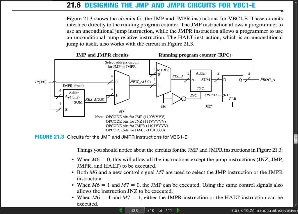
page 488:
· Chapter 22: Designing a Circuit to Prevent Program Execution During Manual Loading for VBC1-E
· Chapter 23: Designing Extended Instruction Memory for VBC1-E
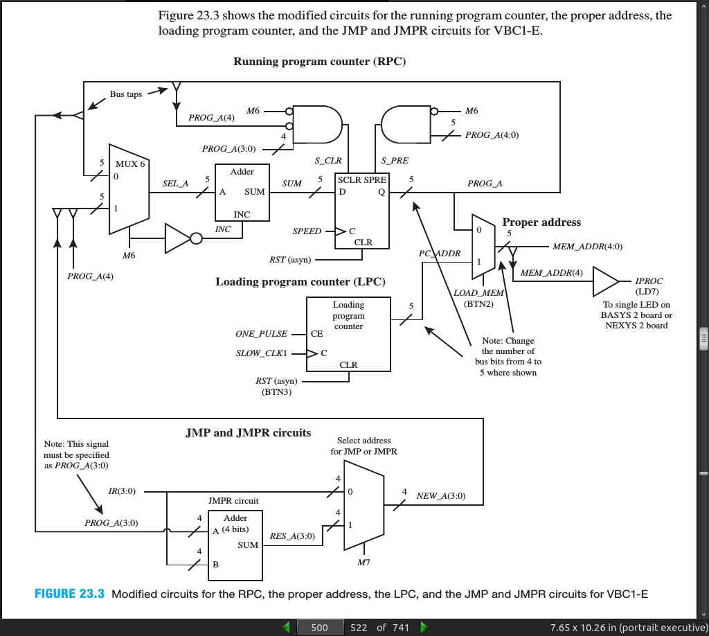
page 500:
· Chapter 24: Designing the Software Interrupt Circuits for VBC1-E
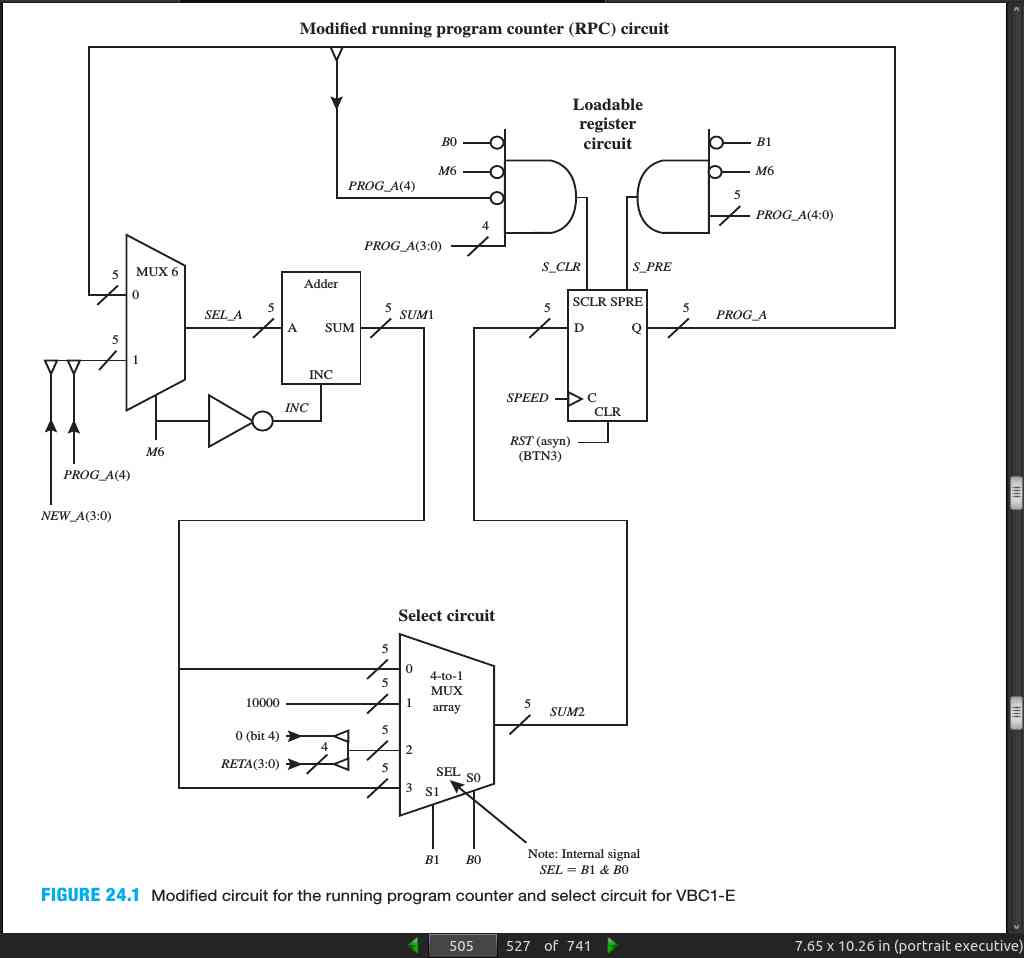
page 505:
· Chapter 25: Completing the Design for VBC1-E
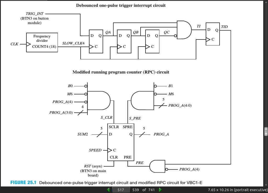
page 517:
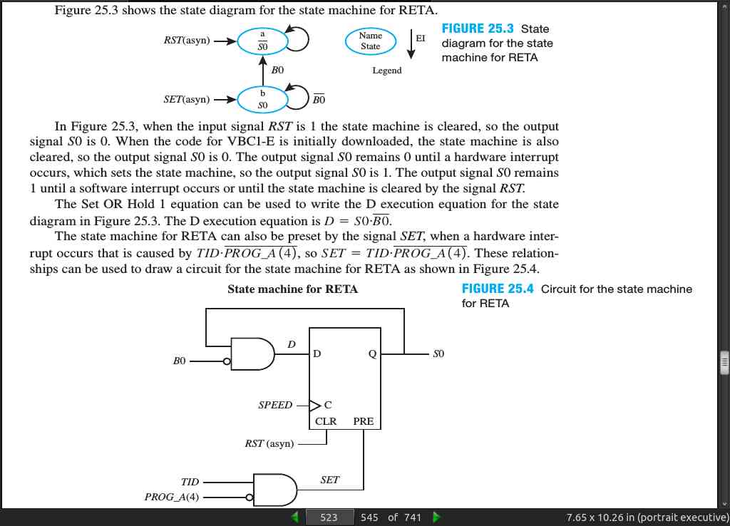
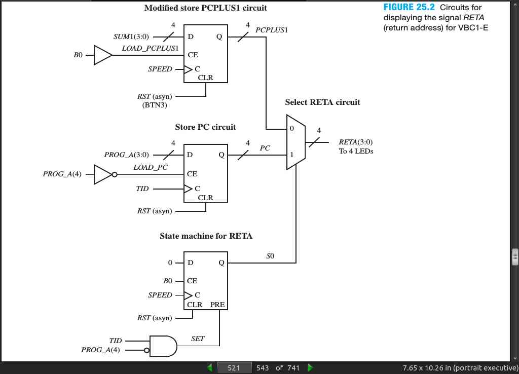
page 521:
page 523: